Getting started with the Analog Discovery Pro 2400 Series
1. Hardware
To set up the ADP2440 or ADP2450:
- First, install the Digilent WaveForms software on your PC. See Installer Details for more information.
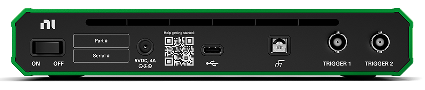
- Connect the device to your PC using a USB cable and connect 5V 4A DC external power supply.
| |
Recommended operating conditions |
Absolute ratings |
| Oscilloscope (1,2,3,4) |
50 V, 1MΩ 10pF or 50Ω |
±50 V or ±5 V (DC + AC peak) |
| Wavegen (AWG 1) |
±5 V, ≤30 mA, 50Ω |
±10 V, 40 mA |
| Digital IOs, Triggers (T1,T2,0,1...15) |
LVCMOS 3.3 V, 4-8 mA, slow-fast |
± 20 V |
| COMPesation |
0/2.5 V, 1 Hz - 1 MHz |
|
| USB |
480 Mbps and 5 Gbps compatible |
|
| Power Supply |
5V, 4A, 20W (typical 2.5A/12.5W) |
4.47V ... 5.46V, 3.483A |
For more information visit the ADP 2400 Series reference page.
2. Software
See Installer Details for information on installing WaveForms.
See WaveForms for information on using the
software.
2.1 System Frequency
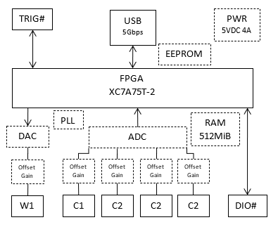
The ADP2440 oscilloscope maximum sampling rate is 600 MHz when only one channel is enabled, 300 MHz when two channels and 150 MHz when 3 or 4 channels are enabled. The data processing runs at 150 MHz.
The ADP2450 oscilloscope maximum sampling rate is 1 GHz when only one channel is enabled, 500 MHz when two channels and 250 MHz when 3 or 4 channels are enabled. The data processing runs at 125 MHz.
The Wavegen (waveform generator frequency) is adjustable in a few steps between 50 and 125 MHz.
The digital frequency for Logic Analyzer and Pattern Generator is adjustable between 50 and 150 MHz. The Logic Analyzer can provide 2, 4 and 8 times higher capture rate, up to 1.2 GHz.
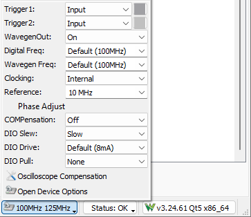
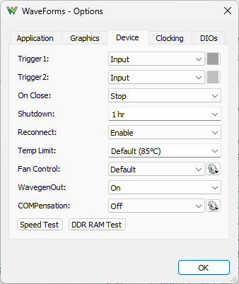
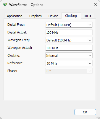
The Trigger channels can be used to output reference clock adjustable between 10 and 25 MHz.
Trigger 1 can be used as 10 ... 25 MHz reference clock input.
To use external reference clock:
- set Trigger 1 to be Input and provide 10-25 MHz
- set Clocking to Trigger 1 Input
- specify the External frequency
To use two ADP2440 or ADP2450 devices together:
- connect Trigger 1 and Trigger 2 between the devices
- in the WaveForms Device Manager select one of the ADP2440 or ADP2450 devices, press "Select + Dual" button and select the other identical device
- the Trigger 1 will be used for reference clock
- the Trigger 2 will be used for instrument synchronization
- The phase of these will be automatically adjusted in the slave device.
To use multiple devices together with separate WaveForms applications, custom application or script:
- connect Trigger 1 between the devices
- on one device set Clocking to output Trigger 1 Output and on the others to be Trigger 1 Input
- configure the same Frequency and External for each device
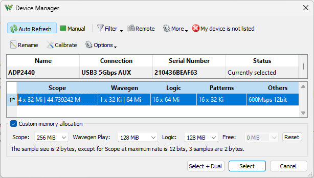
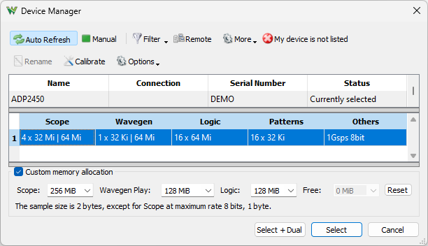
2.2 Memory allocation
The memory allocation between instruments can be adjusted under Settings/ Device Manager.
The Oscilloscope buffer at maximum rates stores samples at 8 or 12 bits, and 16 bits at lower rates.
The Wavegen buffer is only needed to buffer large waveforms for play mode. For shorter waveforms the more flexible 32 Ki samples device buffer should be used.
The Logic Analyzer buffer is usually used with data compression, so normally can store much longer time captures.
3. Troubleshooting
In case you receive the error message "Communication with device failed" or "Device configuration failed":
- Remove all the attached components and wires from the device.
- Verify that the USB cable is attached correctly.
- Try to use a different USB cable and computer plug or hub.
- Try to use a different 5 V DC 4 A power supply.
- Reconnect WaveForms to the device and, without opening any instruments, verify that the WaveForms system monitor is displaying voltage and current levels.
The ADP2440 and ADP2450's system monitor displays the voltage, current, and temperature. In the main window, click the button in the status bar to show this information.
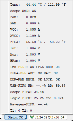
The device typical power consumption is around 12.5W (2.5A) and 2-3W in software shutdown, dimly lit LED. Depending on the usage, consumption can increase subject to the following limitations:
- The supply input is equipped with eFuse power monitor with 3.483 A current limitation. The devices shuts down in order to prevent damage, and the application displays the “Communication with the device failed” error message. The analog circuitry has another eFuse switch with 2.5A limitation.
The LED on the font of the device is:
- dimly lit when powered but not active, indicating power good on the device digital rails.
- fully lit when active, indicating power good on the analog rails.
- fade in/out when in standby mode, device is fully powered but the outputs are stopped. The software is disconnected from the device and OnClose option is Stop.
- blinking on device fault.
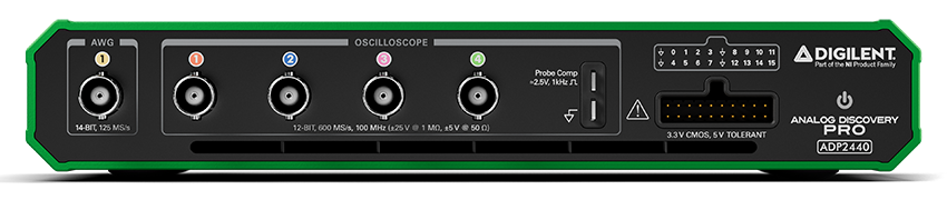
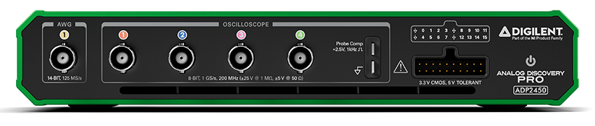
4. Oscilloscope
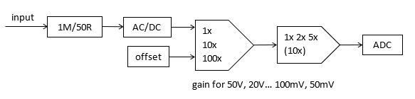
The ADP2440 and ADP2450 have four BNC oscilloscope input channels.
Specifications:
- The ADP2440 oscilloscope maximum sampling rate is 600 MHz when only one channel is enabled, 300 MHz when two channels and 150 MHz when 3 or 4 channels are enabled, at 12 bits. The analog bandwidth is 100 MHz+
- The ADP2450 oscilloscope maximum sampling rate is 1 GHz when only one channel is enabled, 500 MHz when two channels and 250 MHz when 3 or 4 channels are enabled, at 8 bits. The analog bandwidth is 200 MHz+
- At lower rates the samples are stored in 16 bit format which is useful in average sampling mode.
- The channels provide AC or DC coupling option.
- The inputs have an impedance of 1MΩ | 10pF and switchable 50Ω max 5V input termination.
- The peak to peak ranges are the following: 50mV, 100mV, 200mV, 500mV, 1V, 2V, 5V, 10V, 20V, 50V
- The offset DAC is 14 bits ±25 V for 10V range and higher, ±2.5 V for 1 V range and higher, ±250 mV for lower ranges.
- The buffer can be up to 512 MiB samples shared between the enabled channels.
- Each channel can use FIR of 16 taps.
- The bandwidth limitation option is implemented digitally using the FIR
| Peak to peak | Range | Offset |
| 50 V | 5 V/div | +25 V to -25 V |
| 20 V | 2 V/div | +25 V to -25 V |
| 10 V | 1 V/div | +25 V to -25 V |
| 5 V | 500 mV/div | +2.5 V to -2.5 V |
| 2 V | 200 mV/div | +2.5 V to -2.5 V |
| 1 V | 100 mV/div | +2.5 V to -2.5 V |
| 500 mV | 50 mV/div | +250 mV to -250 mV |
| 200 mV | 20 mV/div | +250 mV to -250 mV |
| 100 mV | 10 mV/div | +250 mV to -250 mV |
| 50 mV | 5 mV/div | +250 mV to -250 mV |
- For more information visit the resource center
5. Arbitrary Waveform Generator
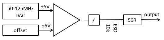
The ADP2440 and ADP2450 is equipped with one Arbitrary Waveform Generator channel.
Specifications:
- The -3dB output bandwidth is 15+ MHz and digital slew rate control is available.
- The output impedance is 50Ω
- The enable/disable option in the Wavegen instrument does not control the output relay but sets to output to 0V.
- The un-powered or shutdown device output is decoupled by a relay leaving the output with 10kΩ pull to GND and ESP protection (402ESDA-MLP1).
The relay can also toggled with WavegenOut option under Settings/Options/Device. The shutdown option also disables the internal Wavegen/DAC clocking.
- The DAC is Texas Instruments DAC5672 14 bits and the rate is adjustable in a few steps between 50 and 125 MHz.
- The maximum output signal swing is 10 Vpk2pk and the recommended output range is -5 V and +5 V.
- The drive current depends on the voltage level, at lest 30 mA and at most 40mA.
- The output buffer is supplied at ±10V so the output voltage can reach close to these values (offset+amplitude) but the recommended usage range is ±5V where it can provide at least 30 mA.
- The DAC resolution is ~0.7 mV for amplitudes above 1 V, and ~0.18 mV for amplitudes of 1 V and lower.
- The offset is controlled by a lower speed 14bit DAC with ~0.7mV resolution with settle time of about 1ms.
- The DC signal in the Wavegen instrument uses the offset. For faster transitions the amplitude should be used, like with stopped square signal and initial output option. By default the application uses animation when selecting a preset value, which could cause output setting in steps. This can be disabled under Settings/Options/Graphics.
- The carrier buffer, AM/PM and FM/SUM buffer size is 32 Ki samples each.
- The play function for longer waveform can use device's DDR RAM buffer to generate at up to 125MS/s.
- For more information visit the resource center
6. COMPensation
The compensation output is by default disabled and can be enabled from status-bar or under Settings/ Options/ Device where the frequency and duty cycle can be adjusted.
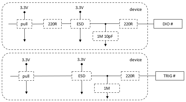
7. Digital I/O
The ADP2440 and ADP2450 has 16 Digital I/O (DIO 0-15) and 2 Trigger I/O channels.
Specifications:
- The channels are supplied at 3.3 V, LVCMOS3V3 standard.
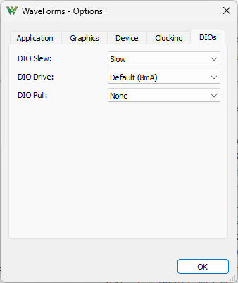
- The drive strength is selectable 4 mA or 8 mA ; slow or fast slew rate.
- Common pull option of about 200uA for all DIO and Trigger IO channels is selectable between: pullup, pulldown, keeper or none.
- The DIOs have a 220 Ω resistor and 220 Ω series PTC thermistor (PRG18BB221MB1RB), 1 MΩ pulldown, 10pF capacitor and ESD diode (DB3S406F) to GND and 3.3V, having protection between -20 V and +20 V. Limiting the output to 8mA and the analog bandwidth is approximately 25 MHz.
- The Triggers have a 220 Ω series PTC thermistor (PRG18BB221MB1RB), 1 MΩ pulldown and ESD diodes (DB3S406F) to GND and 3.3V, having protection between -20 V and +20 V.
- The Logic Analyzer buffer can be up to 256 Million samples / channel, but with data compression, much less is usually needed.
- The Pattern Generator custom buffer is 32 Ki samples / channel.
- The digital frequency for Logic Analyzer and Pattern Generator is adjustable between 50 and 150 MHz. The Logic Analyzer can provide 2, 4 and 8 times higher capture rate, up to 1.2 GHz.
- The Logic Analyzer uses data compression when this is enabled and always for high capture frequencies, like with 100 MHz Digital Frequency at 100 MHz or higher capture rates.