The 34-pin Digital I/O header (J15) brings out the digital input and output signals on the DT7816. To make wiring signals easier, you can attach the STP781x screw terminal panel to this header.
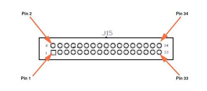
The following figure shows the Digital I/O header (J15) on the DT7816 module.
The following table lists the pin assignments of the Digital I/O header.
Pin Assignments of the Digital I/O Header (J15)
Connector Pin Number |
Signal Description |
Connector Pin Number |
Signal Description |
1 |
General-Purpose Input 0a |
2 |
Digital Ground |
3 |
General-Purpose Input 1a |
4 |
Digital Ground |
5 |
General-Purpose Input 2a |
6 |
Digital Ground |
7 |
General-Purpose Input 3a |
8 |
Digital Ground |
9 |
General-Purpose Input 4a |
10 |
Digital Ground |
11 |
General-Purpose Input 5a |
12 |
Digital Ground |
13 |
General-Purpose Input 6a |
14 |
Digital Ground |
15 |
General-Purpose Input 7a |
16 |
Digital Ground |
17 |
General-Purpose Output 0b |
18 |
Digital Ground |
19 |
General-Purpose Output 1b |
20 |
Digital Ground |
21 |
General-Purpose Output 2b |
22 |
Digital Ground |
23 |
General-Purpose Output 3b |
24 |
Digital Ground |
25 |
General-Purpose Output 4b |
26 |
Digital Ground |
27 |
General-Purpose Output 5b |
28 |
Digital Ground |
29 |
General-Purpose Output 6b |
30 |
Digital Ground |
31 |
General-Purpose Output 7b |
32 |
Digital Ground |
33 |
+5 V (50 mA, maximum) |
34 |
+5 V Return |
a. The input signals are buffered with a
Schmitt trigger gate for noise immunity and are pulled up to 3.3 V with
a 22.1 kW resistor.
The input buffers are operated from 3.3 V
and are 5 V logic tolerant. By default, these signals are configured as
digital inputs.
b. The
output signals are driven by LVTTL buffers and provide 4 mA sink and 10
mA source capabilities.
By default, these signals are configured
as digital outputs.
Using software, you can specify a general-purpose input signal as the signal source for the following destinations:
Digital input (the default signal for each general-purpose input pin)
External A/D trigger input
External D/A trigger input
External A/D clock input
External D/A clock input
Gate input for the general-purpose counter/timer (C/T 0)
Clock input for the general-purpose counter/timer (C/T 0)
Using software, you can specify a general-purpose output signal as the signal source for one of these destinations:
Digital output (the default signal for each general-purpose output pin)
Clock output for the general-purpose counter/timer
(C/T 0)